The 8085 microprocessor is an 8-bit microprocessor introduced in 1976, featuring 16 address lines that allow access to 64K bytes of memory. It includes an accumulator, a flag register, and six general-purpose registers, making it suitable for various computing tasks. This document provides detailed insights into its architecture, pin configuration, and instruction set, making it a valuable resource for electronics students and professionals. Key topics include machine cycles, addressing modes, and interrupt handling, essential for understanding microprocessor functionality.

Key Points

  • Explains the architecture and pin configuration of the 8085 microprocessor.
  • Covers machine cycles and their significance in instruction execution.
  • Details various addressing modes used in the 8085 microprocessor.
  • Discusses the interrupt handling mechanism and its types.
PRAGADHI R
18 pages
Language:English
Type:Textbook
PRAGADHI R
18 pages
Language:English
Type:Textbook
PRAGADHI R
18 pages
Language:English
Type:Textbook
225

8085 Microprocessor Overview and Features pdf

/ 18
8085 Microprocessor Page 1
1.8085 MICROPROCESSOR
1.1 8085 Microprocessor features:
It is invented in 1976.
It is an 8-bit microprocessor.
8085 microprocessor provides 16 address lines, therefore it can access 2^16 = 64K
bytes of memory.
It has 8 Data lines and 16 address lines, out of which 8 address lines are multiplexed
with 8 data lines. Hence it requires external hardware to separate data lines from
address lines (this is one of the disadvantage of 8085).
It generates 8 bit I/O address, hence it can access 2^8 = 256 input ports and 256
output ports.
8085 microprocessor provides one Accumulator, one Flag register, 6 General
Purpose Registers (B, C, D, E, H and L) and two special purpose registers (PC, SP).
The maximum clock frequency of 8085 microprocessor is 3MHz where as minimum
clock frequency is 500 KHz.
8085 microprocessor provides on chip clock generator, therefore there is no need of
external clock generator, but it requires external tuned circuit like LC, RC or crystal.
It is manufactured in NMOS technology
It is available in 40 pin dual in line (DIP) package.
It requires a +5volts of power supply.
8085 microprocessor has five hardware interrupts: TRAP, RST 5.5, RST 6.5, RST 7.5,
and INTR. The hardware interrupt capability of 8085 microprocessor can be
increased by providing external hardware.
8085 microprocessor has capability to share its bus with external bus controller
(Direct Memory Access controller); for transferring large amount of data from
memory to I/O and vice versa.
8085 microprocessor provides two serial I/O lines which are SOD and SID; it means,
serial peripherals can be interfaced with 8085 microprocessor directly.
8085 Microprocessor Page 2
1.2 Pin diagram and Signal Description:
Fig:-Pin diagram of 8085 Microprocessor Fig: - Functional Diagram of 8085
Address & data lines:
Address bus:
8085 has 16-bit address bus AD0-AD7 and A8-A15. In this lower address bus is
multiplexed with data bus. A8-A15 lines are unidirectional and AD0-AD7 lines are
bidirectional.
Data bus:
AD7-AD0 is 8-bit bidirectional data bus. It is multiplexed with lower order address bus.
ALE:
Address latch enable. It is used to de-multiplex AD0-AD7. It is connected to strobe input
of latch which is used to separate address and data bus lines. It is issued in first T-state.
Control & Status Signals:
RD: Read control signal is issued to memory or IO device to read data from it.
WR: Write control signal is issued to memory or IO device to write data into it.
8085 Microprocessor Page 3
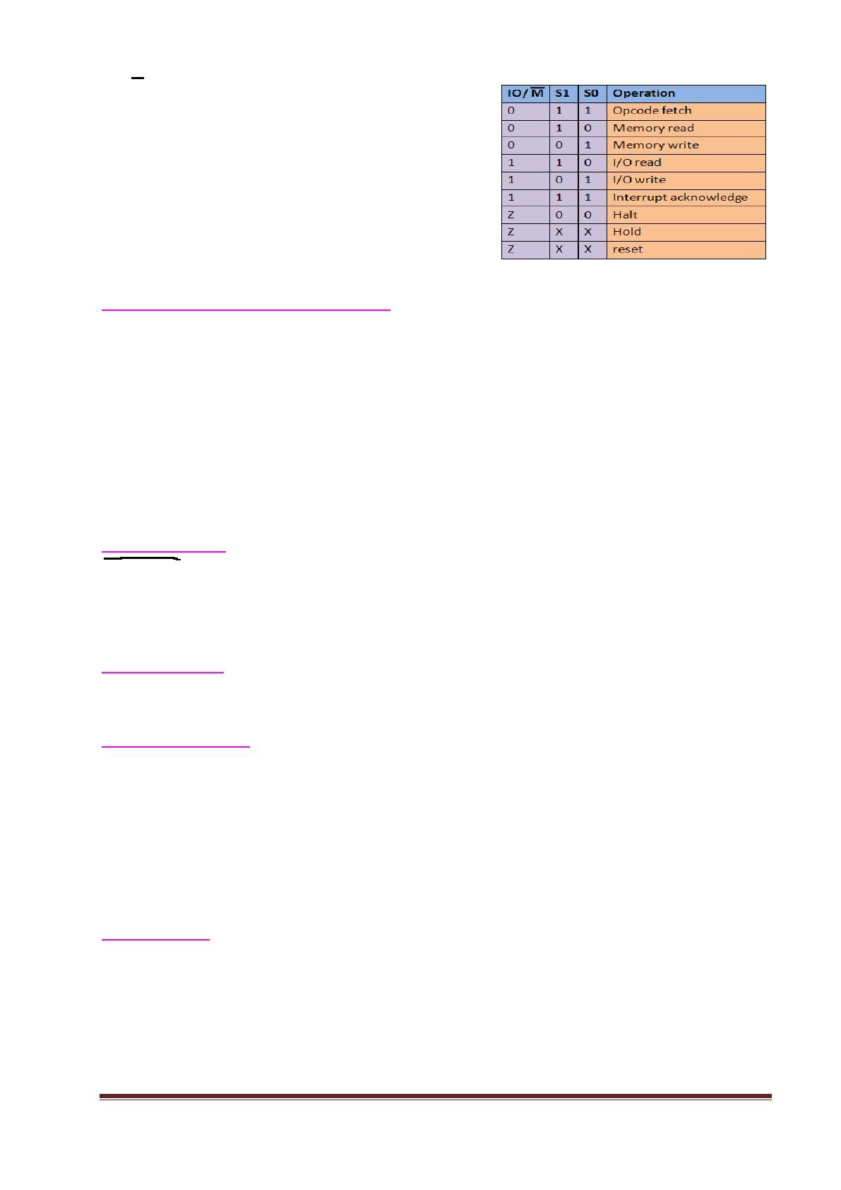
IO/M: It is a signal which is used to distinguish
between IO operation and memory operation. It is
also used in generating memory and IO, read and
write control signals.
S1, S0: These are status signals. Depending on the
value on these lines, the type of operation being
performed by the processor can be determined.
Below table shows that information.
Power Supply and clock signals:
Vcc: +5v power supply line
Vss: Electrical ground signal.
X1, X2: Crystal is connected between these pins. The frequency is internally divided by 2.
The systems operates generally at 3MHz. Hence 6 MHz clock signal needs to be connected
between X1, X2 lines.
CLK (out): It is the clock output signal from processor, which can be used to clock other
peripherals in the microprocessor based system.
READY: This is used when the processor is reading or writing data to a slow peripheral.
When this signal goes low processor inserts wait states, until it goes high.
Reset Signals:
RESET IN: When low signal is applied on this pin, 8085 resets and the microprocessor
boots from 0000h location in memory i.e. PC is loaded with 0000h location.
RESET OUT: When processor is reset, this signal goes high. This pin is connected to reset
input of other peripherals. So when processor is reset, other peripherals are also reset.
Serial IO lines:
SID: serial input data, used to receive serial data.
SOD: serial output data, used to send serial data
Interrupt Signals:
INTR: interrupt request is general purpose interrupt signal. The interrupting device needs
to send the vector address also.
INTA: is interrupt acknowledging signal. This signal indicates that processor has accepted
the interrupt.
RST7.5, RST6.5, RST5.5: These are external vectored interrupts. When these interrupt
occurs, processor vectors to a specific location.
TRAP: It is a non-mask able interrupt.
DMA signals:
HOLD: This line is used by DMA controller to request microprocessor for system bus.
When this line goes high microprocessor completes its current bus cycle and issues system
bus to DMA controller.
HLDA: HOLD acknowledging signal. Processor acknowledges DMA request using this signal.
/ 18
End of Document
225

FAQs

What are the main features of the 8085 microprocessor?
The 8085 microprocessor, invented in 1976, is an 8-bit microprocessor with 16 address lines, allowing it to access 64K bytes of memory. It has 8 data lines and 16 address lines, with 8 address lines multiplexed with data lines, necessitating external hardware for separation. The microprocessor operates at a maximum clock frequency of 3 MHz and requires a +5 volts power supply. It includes one accumulator, one flag register, six general-purpose registers, and two special-purpose registers.
What types of instructions does the 8085 microprocessor support?
The 8085 microprocessor supports a variety of instructions categorized into five functional groups: Data Transfer Operations, Arithmetic Operations, Logical Operations, Branching Operations, and Machine-Control Operations. Data transfer instructions involve copying data between registers or memory locations without altering the source. Arithmetic operations include addition and subtraction, while logical operations involve bitwise manipulation. Branching operations allow for conditional jumps and subroutine calls, and machine-control operations manage the processor's execution state.
What is the architecture of the 8085 microprocessor?
The architecture of the 8085 microprocessor consists of several key components, including an 8-bit Arithmetic Logic Unit (ALU), an accumulator, and a register array with six general-purpose registers (B, C, D, E, H, L). It also features a flag register that contains five flags (S, Z, CY, AC, P) to indicate the status of operations. Additionally, the architecture includes a program counter (PC), a stack pointer (SP), and temporary registers for holding intermediate results during processing.
How does the 8085 microprocessor handle interrupts?
The 8085 microprocessor has five external interrupts, including four vectored interrupts (RST 5.5, RST 6.5, RST 7.5, and TRAP) and one non-vectored interrupt (INTR). When an interrupt occurs, the processor completes the current instruction, disables further interrupts, and acknowledges the interrupt with an INTA signal. The processor then saves the program counter's content on the stack and loads it with the vector address for the interrupt service routine (ISR). After executing the ISR, the RET instruction restores the program counter from the stack.
What are the addressing modes of the 8085 microprocessor?
The 8085 microprocessor supports five addressing modes: Immediate, Register, Direct, Indirect, and Implied addressing modes. In Immediate addressing mode, the operand is specified directly in the instruction. Register addressing mode uses a register to hold the operand. Direct addressing mode specifies the memory address of the operand in the instruction. Indirect addressing mode uses a register to point to the memory location of the operand. Implied addressing mode does not require any operand as the operation is defined by the opcode itself.
What is the significance of the flag register in the 8085 microprocessor?
The flag register in the 8085 microprocessor contains five flags: Sign (S), Zero (Z), Carry (CY), Auxiliary Carry (AC), and Parity (P). These flags are crucial for determining the results of arithmetic and logical operations. For instance, the Sign flag indicates if the result is negative, while the Zero flag shows if the result is zero. The Carry flag signifies if there was a carry out from an operation, and the Auxiliary Carry flag is used in BCD arithmetic. The Parity flag indicates whether the number of set bits in the accumulator is even or odd.
What types of machine cycles does the 8085 microprocessor perform?
The 8085 microprocessor performs several machine cycles, including Opcode Fetch, Memory Read, Memory Write, I/O Read, and I/O Write. Each machine cycle consists of a series of T-states, which are the basic processing steps required to complete an instruction. For example, the Opcode Fetch cycle involves placing the address on the address bus and issuing control signals to read the opcode from memory. Similarly, Memory Read and Write cycles involve placing the address and data on the bus, along with appropriate control signals.